- 您现在的位置:买卖IC网 > Sheet目录3875 > PIC16F628A-I/P (Microchip Technology)IC MCU FLASH 2KX14 EEPROM 18DIP
2009 Microchip Technology Inc.
DS40044G-page 113
PIC16F627A/628A/648A
14.8.1
WAKE-UP FROM SLEEP
The device can wake-up from Sleep through one of the
following events:
1.
External Reset input on MCLR pin
2.
Watchdog Timer wake-up (if WDT was enabled)
3.
Interrupt from RB0/INT pin, RB port change, or
any peripheral interrupt, which is active in Sleep.
The first event will cause a device Reset. The two latter
events are considered a continuation of program
execution. The TO and PD bits in the Status register
can be used to determine the cause of device Reset.
PD bit, which is set on power-up, is cleared when Sleep
is invoked. TO bit is cleared if WDT wake-up occurred.
When the SLEEP instruction is being executed, the next
instruction (PC + 1) is pre-fetched. For the device to
wake-up through an interrupt event, the corresponding
interrupt enable bit must be set (enabled). Wake-up is
regardless of the state of the GIE bit. If the GIE bit is
clear (disabled), the device continues execution at the
instruction after the SLEEP instruction. If the GIE bit is
set (enabled), the device executes the instruction after
the SLEEP instruction and then branches to the
interrupt address (0004h). In cases where the
execution of the instruction following SLEEP is not
desirable, the user should have an NOP after the SLEEP
instruction.
The WDT is cleared when the device wakes up from
Sleep, regardless of the source of wake-up.
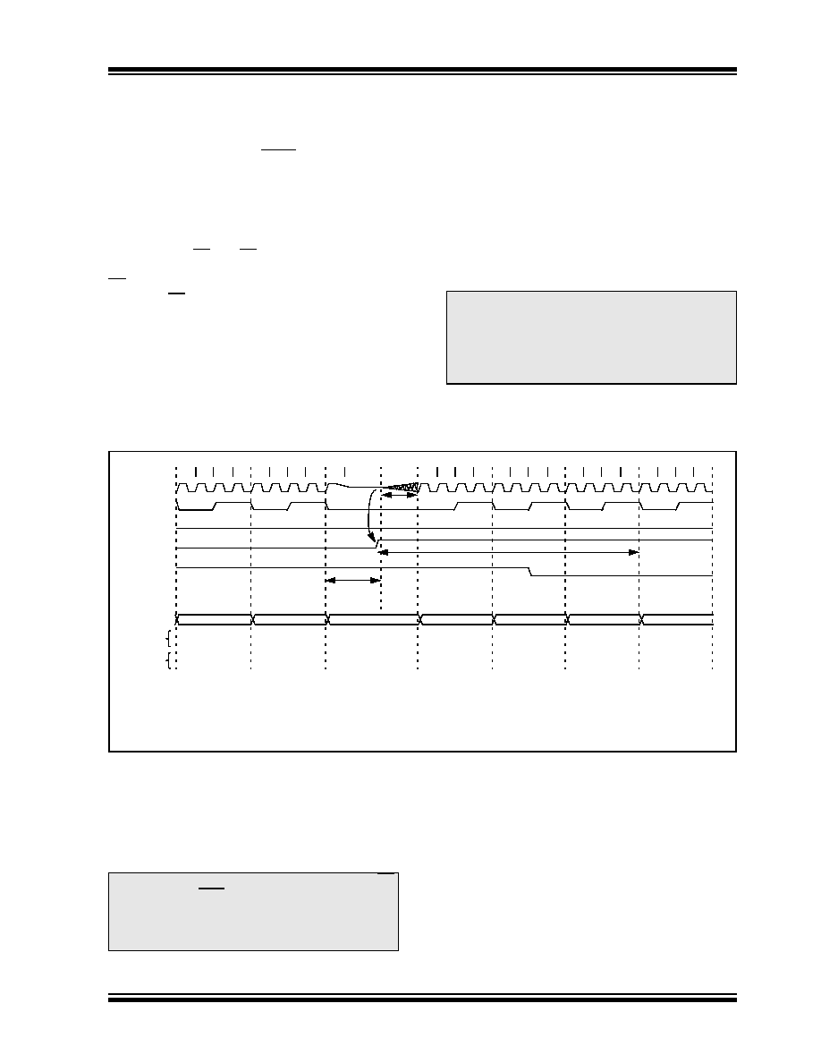
FIGURE 14-17:
WAKE-UP FROM SLEEP THROUGH INTERRUPT
14.9
Code Protection
With the Code-Protect bit is cleared (Code-Protect
enabled), the contents of the program memory
locations are read out as ‘0’. See “PIC16F627A/628A/
648A EEPROM Memory Programming Specification
”
(DS41196) for details.
14.10 User ID Locations
Four memory locations (2000h-2003h) are designated
as user ID locations where the user can store
checksum or other code-identification numbers. These
locations are not accessible during normal execution
but are readable and writable during Program/Verify.
Only the Least Significant 4 bits of the user ID locations
are used for checksum calculations although each
location has 14 bits.
Note:
If the global interrupts are disabled (GIE is
cleared), but any interrupt source has both
its interrupt enable bit and the corresponding
interrupt flag bits set, the device will not enter
Sleep. The SLEEP instruction is executed as
a NOP instruction.
Q1 Q2 Q3 Q4 Q1 Q2 Q3 Q4 Q1
Q1 Q2 Q3 Q4 Q1 Q2 Q3 Q4 Q1 Q2 Q3 Q4 Q1 Q2 Q3 Q4
OSC1
CLKOUT(4)
INT pin
INTF flag
(INTCON<1>)
GIE bit
(INTCON<7>)
Instruction Flow
PC
Instruction
Fetched
Instruction
Executed
PC
PC + 1
PC + 2
Inst(PC) = Sleep
Inst(PC - 1)
Inst(PC + 1)
Sleep
Processor in
Sleep
Interrupt Latency
(Note 2)
Inst(PC + 2)
Inst(PC + 1)
Inst(0004h)
Inst(0005h)
Inst(0004h)
Dummy cycle
PC + 2
0004h(3)
0005h
Dummy cycle
TOST(1,2)
PC + 2
Note
1:
XT, HS or LP Oscillator mode assumed.
2:
TOST = 1024 TOSC (drawing not to scale). Approximately 1
μs delay will be there for RC Oscillator mode.
3:
GIE = 1 assumed. In this case, after wake-up the processor jumps to the interrupt routine. If GIE = 0, execution will continue
in-line.
4:
CLKOUT is not available in these Oscillator modes, but shown here for timing reference.
Note:
Only a Bulk Erase function can set the CP
and CPD bits by turning off the code
protection. The entire data EEPROM and
Flash program memory will be erased to
turn the code protection off.
发布紧急采购,3分钟左右您将得到回复。
相关PDF资料
PIC18F24K22-I/SO
IC PIC MCU 16KB FLASH 28SOIC
PIC18F23K22-I/SP
IC PIC MCU 8KB FLASH 28SPDIP
PIC18LF23K22-I/SP
IC PIC MCU 8KB FLASH 28SPDIP
PIC24F08KA102-I/SS
IC PIC MCU FLASH 8K 28-SSOP
PIC16C58B-20/SO
IC MCU OTP 2KX12 18SOIC
PIC12C672-04/SM
IC MCU OTP 2KX14 A/D 8-SOIJ
PIC18F25K20-E/SS
IC PIC MCU FLASH 16KX16 28-SSOP
PIC18F25J10T-I/SO
IC PIC MCU FLASH 16KX16 28SOIC
相关代理商/技术参数
PIC16F628A-I/P
制造商:Microchip Technology Inc 功能描述:IC 8BIT FLASH MCU 16F628 DIP18
PIC16F628A-I/SO
功能描述:8位微控制器 -MCU 3.5KB 224 RAM 16 I/O RoHS:否 制造商:Silicon Labs 核心:8051 处理器系列:C8051F39x 数据总线宽度:8 bit 最大时钟频率:50 MHz 程序存储器大小:16 KB 数据 RAM 大小:1 KB 片上 ADC:Yes 工作电源电压:1.8 V to 3.6 V 工作温度范围:- 40 C to + 105 C 封装 / 箱体:QFN-20 安装风格:SMD/SMT
PIC16F628A-I/SO
制造商:Microchip Technology Inc 功能描述:8BIT FLASH MCU SMD 16F628 SOIC18
PIC16F628A-I/SOG
制造商:Microchip Technology 功能描述:MCU 8-Bit PIC16 PIC RISC 3.5KB Flash 3.3V/5V 18-Pin SOIC W Tube
PIC16F628A-I/SS
功能描述:8位微控制器 -MCU 3.5KB 224 RAM 16 I/O RoHS:否 制造商:Silicon Labs 核心:8051 处理器系列:C8051F39x 数据总线宽度:8 bit 最大时钟频率:50 MHz 程序存储器大小:16 KB 数据 RAM 大小:1 KB 片上 ADC:Yes 工作电源电压:1.8 V to 3.6 V 工作温度范围:- 40 C to + 105 C 封装 / 箱体:QFN-20 安装风格:SMD/SMT
PIC16F628A-I/SS
制造商:Microchip Technology Inc 功能描述:8BIT FLASH MCU SMD 16F628 SSOP20
PIC16F628AT-E/ML
功能描述:8位微控制器 -MCU 28LD 20MHz 2K FLASH RoHS:否 制造商:Silicon Labs 核心:8051 处理器系列:C8051F39x 数据总线宽度:8 bit 最大时钟频率:50 MHz 程序存储器大小:16 KB 数据 RAM 大小:1 KB 片上 ADC:Yes 工作电源电压:1.8 V to 3.6 V 工作温度范围:- 40 C to + 105 C 封装 / 箱体:QFN-20 安装风格:SMD/SMT
PIC16F628AT-E/SO
功能描述:8位微控制器 -MCU 18LD 20MHz 2K FLASH RoHS:否 制造商:Silicon Labs 核心:8051 处理器系列:C8051F39x 数据总线宽度:8 bit 最大时钟频率:50 MHz 程序存储器大小:16 KB 数据 RAM 大小:1 KB 片上 ADC:Yes 工作电源电压:1.8 V to 3.6 V 工作温度范围:- 40 C to + 105 C 封装 / 箱体:QFN-20 安装风格:SMD/SMT